Video Tutorials
Video Tutorial 1: Overview
of the Fetch operation of a fully functional simple digital computer, the "SIMCO".
Video Tutorial 2 (first half): Tracing the operation
of the "simco" digital computer, logic gate by logic gate, as it follows a computer program to sound an alarm when a window is open.
Video Tutorial 2 (second half): Tracing the operation
of the "simco" digital computer, logic gate by logic gate, as it follows a computer program to sound an alarm when a window is open.
Video Tutorial 2 (End of Part 2): Tracing the operation
of the "simco" digital computer, logic gate by logic gate, as it follows a computer program to sound an alarm when a window is open.
Articles
Programming the SIMCO in Assembly Language
What Is A Computer? Computer Programming, The Purpose of All Computers
Building Simple Machines That Make Decisions
Getting Started Using Programmable Logic Devices
|
Getting Started Using Programmable Logic Devices
This tutorial will help you get started using programmable logic devices.
The simple digital computer described in this website can be built using a Programmable Logic
Device (PLD). Using the CPLD (Complex Programmable Logic Device) design kit from XILINX,
the freely downloadable ISE 9.1i software for programming
the PLD, and Al Williams' introductory tutorial reprinted below and updated to reflect the new 9.1i software, you will have the necessary background
to build the simple digital computer described in this website.
A special thank you to Al Williams of al-williams.com
for generously allowing us to use his article Getting Started With Programmable Logic,
updated for the new ISE 9.1i software.
(Note: XILINX has upgraded their design kit to the new
Cool Runner II starter Kit. The CPLD on this kit is the same one used in the original CPLD design kit I used
to build the simple digital computer. I will eventually be updating this article for use with the newer
design kit.)
Getting Started Using Programmable Logic Devices
by Al Williams
Have you ever wanted to build sophisticated
logic ICs -- not microprocessors, but real digital logic? Sure,
microprocessors let you perform lots of sophisticated logic functions in
software, but sometimes there is no substitute for real hardware.
For example, suppose you have to monitor 16 inputs simultaneously? A
microprocessor can't really watch everything at once and perform other
tasks. It will sample the inputs -- maybe very rapidly -- and there may be
significant delay between an event occurring and the program responding.
You can use interrupts to help minimize this problem, but in the end only
a piece of hardware can do things in a truly concurrent fashion without
resorting to parallel processing.
For the purpose of this discussion, I'll talk about programmable logic
devices (PLDs) as a broad category of ICs that can be programmed by the
user to perform different functions. These aren't software programmable
ICs like microprocessors, though. In practice, there are several types of
PLDs including CPLDs (complex PLDs) and FPGAs (field programmable gate
arrays). From our point of view, all these chips are basically the same,
and differ mainly in the complexity of circuits they can mimic and
price.
The general idea is simple:
 |
You describe the circuit you want to
build using schematics or a programming-like language. In many
cases, you'll use both methods in a single
project. |
|
Tools provided by the PLD maker
allows you to simulate the design on your workstation. When it works
in simulation, you can have a high degree of confidence that the
design will work in real life. |
|
The tools then compile your design to
a bit stream that you can program into the chip and you have a
customized chip. Modern PLDs can be programmed many times. |
It is important to realize that these bit streams are not programs in
the sense of a sequential list of instructions. PLDs contain hundreds or
thousands of logic gates and flip flops. They also provide a huge
programmable interconnecting switch. The workstation software figures out
how to connect the internal gates to match the logical description of your
circuit. The program sets the "wires" between the internal gates.
Of course, the final result might not look like what you specified, but
the result should be the same. For a hypothetical example, suppose you
design an AND gate. However, suppose your PLD only contains NAND gates.
Your design might look like this:

The final implementation might really look like this:

The software figured out that it could make an AND gate from
a NAND gate with another NAND serving as an inverter. Of course, this is a
simple example. A CPLD might model a few thousand gates and some FPGAs are
much larger than that! With a large enough chip, you can even custom
design a CPU!
PLD Road Map
So PLDs sound great, right? Why doesn't everyone use
them? There are a few challenges you have to overcome. First, most PLDs
are in packages that are hard to work with. Second, until recently, most
PLDs required expensive development hardware and software.
Luckily, AWC has the answer to these problems. We have a low-cost PC
board that allows you to easily work with several Xilinx PLDs. Another
board allows you to program the PLD with your PC's printer port (you only
need one programmer board). The board can accept breadboard wires, or you
can use the board to connect your own prototypes by soldering wires in
where the usual kit has sockets. Finally, you can get great design
software free from the Xilinx Web site.
This tutorial will take you through a simple design with the Xilinx
software and our PBX84 board. Of course, you could use any Xilinx
development board, but you won't find one that is easier to use or less
expensive than the PBX84.
For a simple example, I'll show you how to construct this half-adder
design.
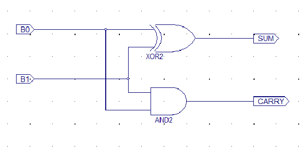
This simple circuit takes two bits, B0 and B1, and adds them producing
a SUM and a CARRY output.
Before you start, you need to install the Xilinx Web Pack software on
your PC. Since it can simulate your design, you don't need any hardware to
see the results, although if you want to implement the actual hardware,
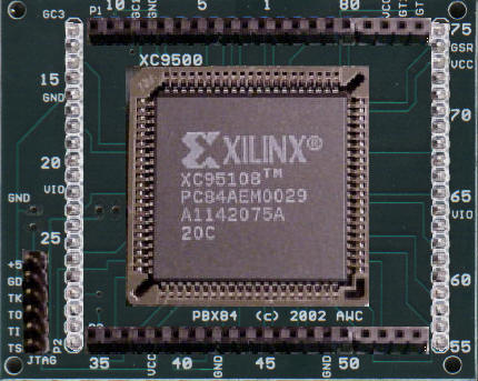
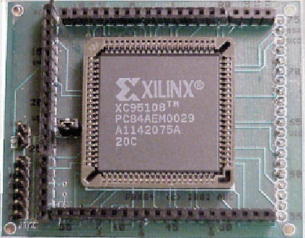
you will need a Xilinx XC9500-series PLD, a PBX84, and the matching
programmer.
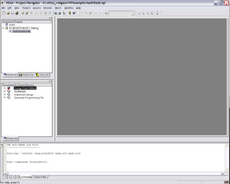
Starting the Half Adder
After installing the ISE 9.1i software, a Xilinx ISE 9.1i icon will be placed on your desktop.

Double click on this icon to start the ISE 9.1i Project Manager, shown below.
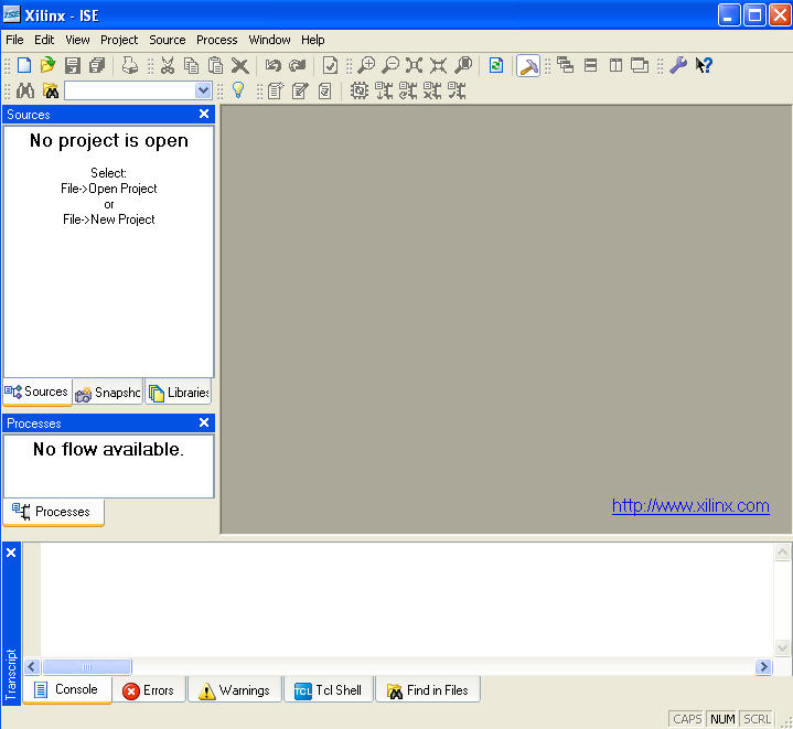
When you
start the Project Manager you'll see a blank work area. The first
thing you want to do is create a new project (File | New Project on the
menu). You'll see a dialog box:
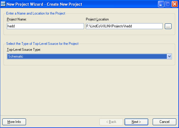
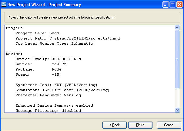
I'll name the new project hadd. The location gets set automatically,
although you can change it if you like. Be sure to select schematic as
the Top-Level Source Type. Click the Next button to continue.
The Device Properties window will appear, as shown below:
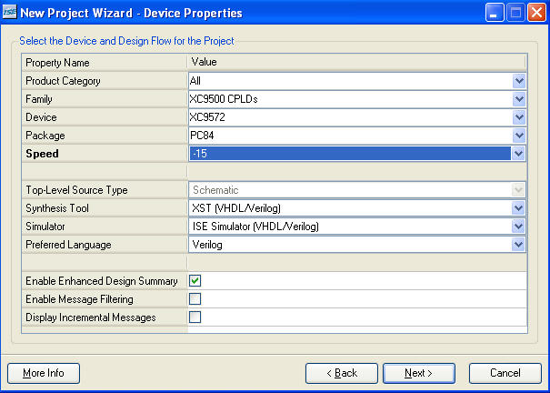
The device we will be using is the XC9572 XILINX CPLD. We want the
XC9500 CPLDs family, the XC9572 device, the PC84 package, and the
XST (VHDL / Verilog) Synthesis Tool.
Select the options shown in the picture above and click the Next button to continue.
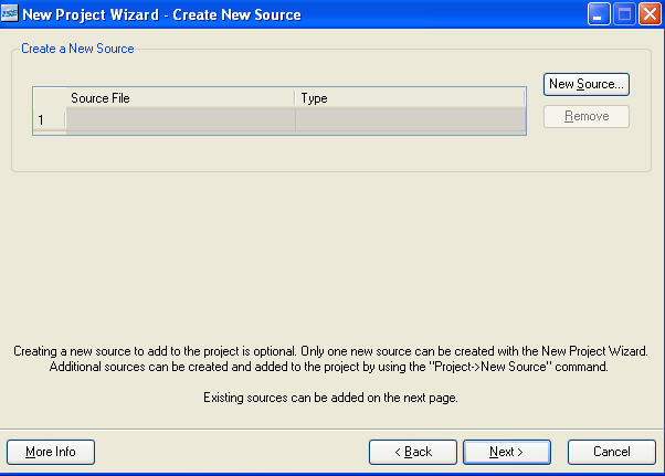
The Create New Source window will appear. Click the New Source button to add a new source file.
This brings up a dialog where you can
pick what kind of design file you want to create:
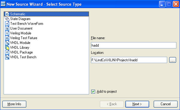
Obviously, you want to select "Schematic" as the document
type. I named the file hadd, since this will be the top-level design file.
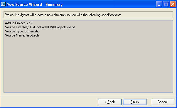
Press Next. You'll see a New Source summary screen; just press Finish.
You will be presented with a second Create New Source window. Simply click the Next Button, do not add a new source.
The Project Summary screen will appear. Click Finish.
This will
bring up the schematic editor, which is a different program.
Now you are ready to draw the schematic. On the left hand side of the
schematic editor, you'll see a window that contains categories and
symbols. The symbols we want are in the Logic category and are named xor2
and and2 (a two input xor and an and gate, as you might guess). Select
each gate, move the mouse over the schematic area, and click to drop the
gate. Then you can use the Add Wire command (or the Add Wire tool button
near the top of the window) to draw the connections. Your final result
should look like this:
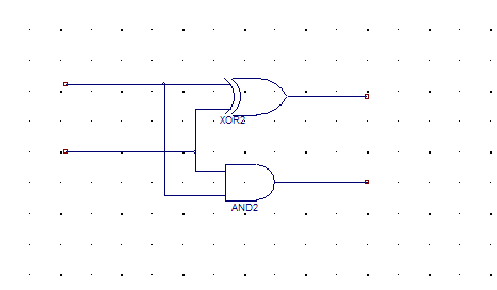
Notice that the outputs have short wire stubs drawn from
them. This is necessary since you can't put an I/O marker directly on a
gate output. You'll add I/O markers to the wire stubs in the next
frame.
When you are drawing a wire, you can double click to end the
wire without dropping the tool. This is especially handy when drawing the
wires to nowhere.
Incidentally, you can find Xilinx's complete documentation
(some of which doesn't apply to the Web Pack) at http://toolbox.xilinx.com/docsan/xilinx4/manuals.htm.
Adding I/O
Next,
select the Add I/O Marker command from the menu (or the toolbar; or press
Control+G). Near the top of the screen you will see three radio buttons
appear: Input, Output, and Bidirectional. Select Input and click on the
two inputs. You have to click just at the ends of the wires or else the
I/O marker won't "drop" and you'll have to try again. Switch to Output and
drop the two output markers.
Remember, you can't drop an I/O marker directly on a gate input or
output. In the drawing below, for example, you must draw wire "stubs" from
the gate outputs so you can drop a marker.
These new markers will have automatically generated names that make no
sense. Double click each marker and change the node names to match this
drawing:
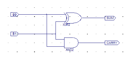
And you are done! Before you leave this frame, press Tools |
Check Schematic check your design. You should get no errors. If you do get
errors, fix your problems before you continue. Common errors occur when
you fail to connect items, or have multiple connections made
incorrectly.
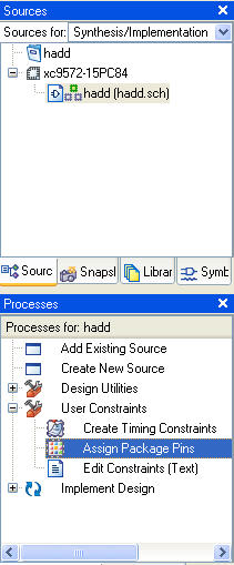
Switch back to the Project Navigator. We need to assign the
I/O markers to physical pins (constraints in Xilinx terminology). If you
don't care, you can omit this step and let the compiler pick pin numbers
for you. However, most often, you have a circuit in mind and you want to
fix these I/O markers to particular pins.
For this design I'll use pins 70 and 71 for sum and carry.
B0 and B1 will be on pins 61 and 62. Make sure hadd is highlighted in the
Sources in Project window. In the lower window click the plus sign next to
User Constraints.
Double click Assign Package Pins.
The dialog window below will appear:
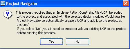
Click Yes to allow a UCF file to be added to the project.
This will open the ChipViewer
window:
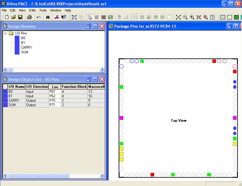
You may need to zoom in (with the + icon on the toolbar),
and resize the window to see everything clearly. Also, you'll need to
click the plus signs in the Signals column to see all the inputs and
outputs.
Just click on an input and then click on the corresponding
pin. Repeat for the remaining inputs and outputs. That's it! Use File |
Save to save the file, close ChipViewer, and switch back to the Project
Navigator.
Get Ready...
The next step is to compile your design and program your chip. If
the design were more complex, you might want to simulate it first, but
we'll put that off for a later frame.
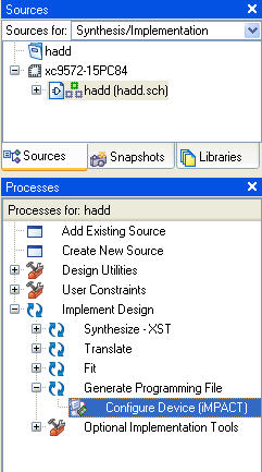
The Process Viewer has several entries:
|
Design Entry Utilities - Tools for
entering your design (for example, ChipViewer). |
|
Synthesize - Compiles design files. |
|
Implement Design - Takes compiled
files and "fits" them to your selected device. |
|
Generate Programming File - Create a
file to download to the device. |
The Project Navigator is smart enough to perform any prerequisite steps
before performing a requested action. Therefore, you can simply double
click Configure Device (iMPACT). This will do all the compilation steps
required and then launch iMPACT to program your chip. The iMPACT manual is
available on the Web, but unless you are doing something other than just
programming the chip, you'll probably never need it.
The Welcome To Impact screen will display:
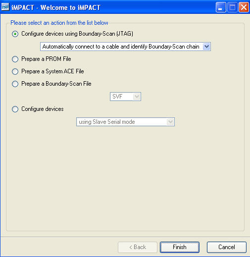
Select the Configure devices using Boundary-Scan(JTAG) option
and select the Automatically connect to a cable and identify Boundary-Scan chain from the drop down list.
You should have the JTag programming board connected to your PC via a
parallel port cable and the board should be plugged into the PBX84
(consult the PBX84 manual). The boards must have power applied. Click Finish.
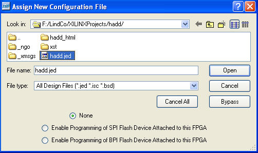
The Assign New Configuration window will display. Select the file name hadd.jed and click Open.
The iMPACT
program should detect your JTag cable and show you a graphic
representation of your device:
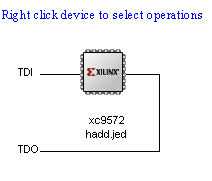
Right click on the chip and select
Program. This shows you this dialog:
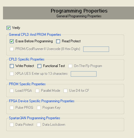
Make sure that the Verify and Erase Before Programming options are checked, then click OK. The operation takes a little while before
the progress bar starts to move (15-30 seconds):
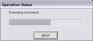
Once it starts moving, the operation completes quickly. The chip begins
operating as soon as programming is complete. You'll want to connect pins
70 and 71 to LEDs through appropriate resistors (220-470 ohms). You'll
connect pins 61 and 62 to pull up resistors and use a switch or wire to
ground to set them to the zero state.
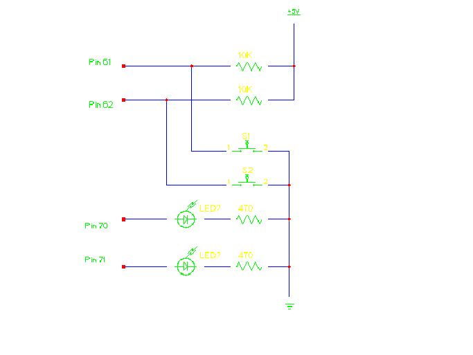
Note: The previous version of this figure had the pin numbers
reversed. It really doesn't matter which pins you use as long as you set
your constraints to match (see the last frame).
You should be able to manipulate the switches (or breadboard wires) and
see that:
0 + 0 = 0 0
0 + 1 = 0 1
1 + 0 = 0 1
1 + 1 = 1 0
Congratulations! You programmed a CPLD!
|

Jen has a Bot.
Bit the Bot.
If Bit is On, He Can Do (and say) A Lot!
Coming Soon...
Meet Bit the Bot, a talking robot that convinces us of our own, true, spiritual nature...
and who opens minds to be receptive to the Gospel message of salvation through Christ Jesus.
Talk to Bit the Bot soon about his adventures with Jen and Ben at www.JenAndBit.com
|